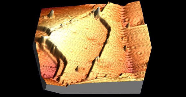
 Like the surface of an alien planet, thin sheets of copper display a complex topography of ridges and valleys. These never-before-seen undulations may spell trouble for electronic gadgets: The zigzagging surface could contribute to the electrical resistance of miniature copper wires that snake throughout computer chips.
Using a scanning tunneling microscope, scientists observed nanoscale peaks and dips on a sheet of copper, with angles of a few degrees, researchers report in the July 28 Science. “When we saw that, we were absolutely shocked,” says materials scientist John Boland of Trinity College Dublin. Conventional wisdom was that the copper would lay mostly flat. Copper and other metals are a conglomeration of smaller bits, known as grains. Within each grain, the atoms are neatly arranged, but at grain boundaries, the pattern is disrupted. In the type of copper the researchers studied, nanocrystalline copper, the grains are particularly small; each has around 1 million atoms. Boland and colleagues showed for the first time that, in films of nanocrystalline copper just tens of nanometers thick, peaks and dips appear where misaligned grains meet. Read Article: https://www.sciencenews.org/article/thinnest-films-copper-look-flat-they-arent Comments are closed.
|
About Oliver Briscoe
Oliver Briscoe is a 20+ year veteran of the Informational Technology field. He understands his first principals and loves teaching others. Archives
October 2017
Categories
All
|
 RSS Feed
